


Design of depth gain compensation circuit for ultrasonic sensor
0 quote
As an important method in the field of railway locomotive and vehicle maintenance, ultrasonic nondestructive testing plays an important role in ensuring the safety and stability of the performance of components. However, the currently widely used simulation ultrasonic testing equipment has been unable to meet the testing requirements of the rapidly developing rail vehicles and their components. Therefore, the digital, intelligent and miniaturized ultrasonic testing system is researched and designed. It is of great practical significance to expand the application of ultrasonic detection technology in the field of railway locomotive and vehicle.
Whether it is analog or digital ultrasonic flaw detector, it is sent out by ultrasonic sensor ultrasonic signal of a certain frequency, when the ultrasonic wave propagates in the actual medium, it will produce attenuation. In order to compensate the energy loss caused by scattering attenuation and absorption attenuation of echo signals lost with the increase of propagation distance, and reduce the error of injury detection, for the propagation medium with the same nature, amplifier gain must be carried out on the echo signal according to the depth or the length of wave propagation time, so that the defect signals with different depths show the same amplitude.
In order to solve the problem of signal attenuation, it is necessary to design a circuit that can flexibly control the gain multiple of amplified echo signal, so that the defect shows the same amplitude at any depth. Therefore, compared with the traditional analog circuit, the gain range and timing accuracy can be controlled more flexibly by using field programmable gate array (FPGA) digital controllable gain circuit and PLL digital phase-locked loop management module, which makes it possible to control analog amplification by digital means.
1. System overview and block diagram
The handheld EMU bogie ultrasonic flaw detector system takes the ultrasonic probe as the sensor, and Xilinx XC6SLX16 FPGA as the main control and processing chip, as shown in Figure 1. The working process of the system is as follows: when the system is powered on, FPGA communicates with the upper computer through the communication interface, receives the command to start acquisition from the upper computer, and initializes through the parameters stored in the Flash. If, open the transmitting circuit of the ultrasonic probe, let the receiving circuit receive the echo signal, and set the repeat pulse frequency. After the high-voltage power supply generates high-voltage narrow pulse through the excitation and emission circuit of the excitation module, the piezoelectric wafer of the ultrasonic probe is excited to generate ultrasonic wave. After the ultrasonic wave propagates inside the workpiece to be measured, surface echo, defect echo and bottom echo will be formed. After the echo signal with three kinds of signals enters the acquisition and preprocessing module through the receiving circuit, the depth gain compensation will be carried out. And the amplifier circuit amplification pre-processing, then into the processing and display module, digital filtering, digital detection, data compression and other reprocessing, finally through the F1 series chip and the upper computer USB to UART/FIFO conversion communication, display the detection results on the upper computer.
2. Depth gain compensation principle and circuit design
2.1 Depth gain compensation principle
In the far field region of the wafer, the farther the distance is, the lower the amplitude of the echo wave will be. This is caused by the attenuation of the acoustic beam expansion and sound in the material. Therefore, different degrees of compensation gain are needed for echo electrical signals of different depths, which is the purpose of the depth gain compensation circuit. That is to say, the electronic method is used to compensate the defect of the same size at different depths, so that the echo amplitude of the echo signal in the far field area has roughly the same echo amplitude in the coordinate system. In this way, the echo signal in the far field area has basically the same amplitude as that in the near field area, so that the defect in depth cannot be judged due to the large attenuation of signal strength due to the long distance in the far field area. Misjudgment and missed judgment. With the increase of ultrasonic transmission distance, the total energy will gradually show exponential attenuation. Therefore, it is necessary to make compensation gain for weak (usually grade A) reflected echo signals of different depths and amplify them by the amplifier circuit, so as to facilitate further processing and display by the post-stage module. The principle is shown in Figure 2.
FIG. 2(a) and (b) are the schematic diagram before compensation, and FIG. 2(C) and (d) are the schematic diagram after compensation. It can be seen that, after depth gain compensation, defects at different depths of the workpiece to be tested will show the same amplitude through type A display method, which will not cause insufficient equivalent display and misjudgment due to attenuation.
Generally speaking, for plane cosine waves, the attenuation rule of sound pressure can be expressed as

Where P. Is the sound pressure when incident on the material interface; P is the sound pressure after the ultrasonic wave propagates in the material for some distance a; Is the attenuation coefficient.
It should be pointed out that, for most solid and metallic media, the ultrasonic attenuation commonly referred to, that is, the attenuation characterized by o/(attenuation coefficient) includes scattering attenuation a and absorption attenuation, which can be obtained from common formula (1) if the ultrasonic wave propagation back and forth is specified as 20
It can be seen from formula (3) that the ultrasonic propagation distance is related to the inherent propagation rate and time t in the propagation medium. When the workpiece to be measured is determined, the attenuation coefficient and propagation rate will not change. Therefore, the decibel number of the ultrasonic amplitude reduction in the propagation distance is directly proportional to the propagation time t. The number of decibels of amplitude to be compensated is directly related to the propagation time. The depth compensation gain is also called the time compensation gain.
2.2 Application design of depth gain compensation amplifier circuit
The depth compensation amplifier circuit is mainly composed of DAC902, rail to rail operational amplifier OPA350 and D/A converter chip AD8330. The digital input part of the DAC902 chip is completed by FPGA, and the IP core of FPGA generates the DCM clock management module, and uses the PLL digital phase-locked loop to generate the precise clock signal needed by the DAC902 chip. Under the clock signal, DAC902 generates time sequence and starts D/A conversion. When D/A conversion is completed, the output variable voltage is input to the input end of the variable gain amplifier AD8330. The depth gain compensation function can be realized according to the linear relationship diagram between the input voltage and the compensation gain.
DAC902 is A high speed D/A converter with 12-bit resolution capability, low noise and low power consumption. Its sampling rate can reach up to 165MSPS, and its data port is parallel, which facilitates communication with FPGA. It has a high current output impedance (200 Ki1) with a 20mA nominal range and an output conforming up to 1.25 V. The differential output allows for a differential or single-ended analog signal interface, and the closely matched current output ensures excellent dynamic performance in differential configurations. In the circuit shown in Figure 3, its 12-bit DA data input terminal is connected to the pin of XC6SLX16, the power terminal is filtered by the capacitor, and the digital ground and the analog ground have been well isolated. The CLK terminal is connected to the FPGA pin, where a 5O % duty cycle signal is used to meet the performance needs of high-speed conversion. Because DAC902 is special, there is no signal input at the enable end of the chip, so it can be seen from the sequence diagram: Its data reading and conversion are completed by clock control, which is more important for FPGA to produce accurate clock control. Compared with other microcontrollers, FPGA is more capable of generating clock signals with minimal accurate errors, cooperating with timing sequence, and reducing flaw detection errors.
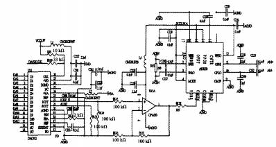
Figure 3. Design of depth gain amplifier circuit
As can be seen from the analysis of Figure 3, the output current i of DAC902 is in differential form. After resistance matching, the voltage is divided into the voltage feedback operational amplifier OPA350. The amplified voltage signal from the operational amplifier is fed into the pre-variable gain amplifier AD8330 for depth gain compensation. After that, the analog output signals enter the LTC2249 chip for A/D conversion, and then connect with the FPGA to complete the digital signal processing task. The supply of compensating voltage of AD8330 is realized by DAC902. The output voltage algorithm of DAC902 is as follows:


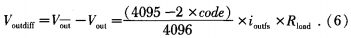
As can be seen from the calculation results of Formula (6), the output voltage of the DAC902 is mA level. Therefore, it is necessary to amplify the voltage by the OPA350 operational amplifier of the later stage to the RMS voltage allowed at the voltage input terminal of the later stage AD8330 to make the analog chip work normally. At this time, FPGA needs to follow the depth compensation principle. As shown in Figure 2, distant echo takes a long time to reflect to the receiving circuit, while close-range echo takes a short time to reflect to the receiving circuit. With the increase of time, digital signals with changing values from small to large can be generated to control DAC902 to generate constantly changing voltage signals. Then control the gain amplifier circuit device AD8330 to the input weak echo signal analog depth gain compensation. In addition, the OPA350 is a rail-to-rail CMOS operational amplifier. In order to suppress noise in the circuit and prevent the power from entering into noise signals, two bypass capacitors are added to the incoming line of the power supply for filtering. In addition, since the input impedance of AD8330 R=100Q, The front-end amplifier OPA350 was added to improve the input impedance and increase the matching ability of the back-end circuit.
AD8330 is a low power, voltage control type variable gain amplifier, compared with AD603, AD8331 has a larger constant bandwidth of 150MHz, its basic gain range is 0-50dB, the highest value can be increased by 20dB(i.e., 20-70dB), the lowest value can be reduced by 30dB(i.e., -30 +20dB). Thus providing an unprecedented 100dB gain range.
2.3 A/D conversion circuit
After the processing of the depth gain compensation amplifier circuit, the echo analog signal enters the LTC2249 by AIN± pin, and starts A/D conversion. The converted digital signal is input into XC6SLX16, and then a series of algorithms such as digital signal processing, digital filtering, detection, digital compression and sampling are carried out for communication with the upper computer. Display more clear information about the injury. The circuit schematic diagram is shown in Figure 4
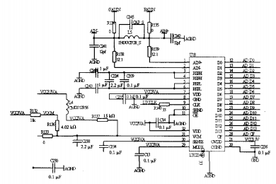
Figure 4 A/D conversion circuit design
The LTC2249 is a L4-bit 8OMSPS, low-power 3VA/D converter designed for digital processing of high frequency, wide dynamic range signals. A single-ended clock input pin is used by the FPGA's DCM clock management module to control the timing operation of the converter, where the optional clock duty ratio stabilizer provides high performance conversion rates in conjunction with the preceding variable gain amplifier circuit at full speed over a wide clock duty ratio range.
3. Experimental results and analysis
In this circuit, the idea of the experiment is: using the function signal generator to send the sine wave signal to the receiving end of the circuit board of the ultrasonic flaw detector, observe the output waveform on the upper computer interface and judge whether the design of the depth gain compensation amplifier circuit meets the design requirements.
The USB to UART/FIFO conversion circuit chip FT2232 completes the interface communication between FPGA and the upper computer. After the ultrasonic echo signal simulated by sine wave is transmitted to the upper computer through the depth gain compensation circuit, the waveform can be observed in the display interface area after a series of processing by the upper computer software. Here, a sinusoidal wave with a frequency of 5MHz and a peak-to-peak value of 2mV is sent to the flaw detector. When the initial gain value is set to 34dB, three different gains with a step of 5dB are set, and the amplitude changes are observed.
4 Conclusion
XilinxISE12.3 integrated development environment is used to complete the input, simulation and synthesis of the depth gain compensation program. After verification by Testbench, combined with the circuit design, debugging is done on the circuit board to achieve the purpose of communicating with the upper computer. Finally, the design requirements of the depth gain compensation amplifier circuit are realized.
The experimental results show that: After adding sinusoidal excitation with frequency of 5MHz and peak-to-peak value of 2mV into the input end of the circuit, three different gains of 5dB are set on the upper computer, and the amplitude changes are observed. The sinusoidal signal amplitude received from the upper computer increases by l times, which indicates that the ultrasonic flaw detector can collect and transmit smoothly and display signals on the upper computer. Achieve different amplification gain, so that the attenuation is compensated.
References:
[1] Shen Jianzhong, Li Lian-xiu. Development of Ultrasonic Nondestructive Testing [J]. Non-damage detection, 1988, 2O(2) : 31-33.
[2] Chang Qinglong. Development of Hardware System for Ultrasonic Wave automatic Damage Detection Based on ARM Platform [D]. Nanjing: Nanjing University of Aeronautics and Astronautics, 2008. (in Chinese)
[3] Huang Zhiyuan, Wang Aiguo, Huang Zhongcan. Improvement of TGC Circuit of Ultrasonic Diagnostic Instrument [J]. Journal of Wuhan University of Science and Technology, 2005(8) : 30-32.
[4] Wang Xiaofeng, Zhou Jipeng. An online FLASH Configuration Method based on FPGA [J]. Electronic Devices, 2006(9) : 902-904,908. (in Chinese)
[5] Xie Haixia, Sun Zhixiong. FPGA implementation of multiphase Extraction Filter [J]. Electronic Parts, 2012(6) : 331-333.
[6] Liu Chengming, Zhang Yanbing, Li Xine. Real-time lossless data compression System Design based on FPGA [J]. Technology Review, 2011(7) : 28-29.
[7] Chen Xiaodong, Fu Yongqiang, Wang Xiaohua, et al. Design of Band-pass Filter for Ultrasonic Augmentation Compensation [J]. Research and Development, 2007(5) : 43-45.
[8] Editing and Reviewing Committee of Training Materials for Qualification and Certification of Nondestructive Testing Personnel in National Defense Science and Technology Industry. Ultrasonic detection [M]. Beijing: China Machine Press, 2007.
[9] Zhang Ke, Yu Guohua, Liu Ganghai. Research on Echo signal processing method of ultrasonic wave Ranging [J]. Measurement and Control Technology, 2008,7 (1) : 48-50.