


Simulation calculation and optimization design of SOI monocrystalline silicon pressure sensor
The pressure sensor made of semiconductor silicon (including monocrystalline silicon and polysilicon) is an important part of the whole sensor. With the development of information technology, people put forward higher and higher requirements for the working temperature of sensors. A variety of high-temperature pressure sensors have been studied abroad since the late 1980s. But no matter which kind of sensor, the strain film stress distribution is closely related to the performance of the sensor, the selection of appropriate strain film size, thickness and strain resistance on the strain film arrangement position becomes the key to the design of the sensor. This paper mainly uses ANSYS finite element analysis method... The simulation of multilayer strain film for SOI monocrystalline silicon high temperature pressure sensor is carried out. Firstly, the relative errors of the strain film thickness ratio are calculated and compared. Theoretically, it is pointed out that it is unnecessary to simulate other film layers on the surface of bulk silicon under the general accuracy requirement. Secondly, the theoretical output of strain film with different width-length ratio and different thickness is simulated, and the optimal selection scheme of strain film is discussed. Finally, according to the simulation results, the SOI monocrystalline silicon high temperature pressure sensor was designed and developed for the first time, and the measurement was carried out. The simulation optimization scheme was verified experimentally, and the measurement results were in agreement with the theoretical values.
1 SOI monocrystalline silicon high temperature pressure sensor
The SOI(Silicon-on-Insulator) high temperature and pressure sensor is a combination of SDB(silicon-silicon direct bonding technology) and the concentrated boron self-stopping corrosion technology. The structure is monocrystalline silicon as substrate and strain resistance, and silica dielectric layer is used as isolation between them. It not only uses the high strain factor of monocrystal silicon to improve the sensitivity of the sensor, but also uses the dielectric isolation instead of P-N junction isolation to reduce the leakage current and improve the working temperature of the sensor. At the same time, the repeatability of monocrystalline silicon is utilized in the process, which is fully compatible with CMOS process.
2 Introduction to ANSYS
The stress simulation software we use is Ansys produced by ANSYS Company, which is a special software for finite element analysis. With the help of it, designers do not have to engage in heavy calculation or their own programming, or even do not have to understand the details of finite element analysis, as long as they master the usage of the software, and can express their ideas accurately to it, they can get the required results, greatly improve the work efficiency, reduce the work burden of the designer. We used ANSYS/Muhiphysics/Ls-Dyna 6.0 software to write this article.
3. Rationality of sensor simplified stress model
In order to make the designed sensor more reasonable, with as high sensitivity as possible, the stress analysis of the sensor must be carried out first, only in this way can the correctness of the design be guaranteed theoretically. The traditional design is based on theoretical calculation of strain membrane design. With the application of CAD tools, computer aided design can save a lot of trial production time, reduce the cost of trial production, and make the product more competitive. However, in the current stress analysis of silicon pressure sensor, whether theoretical analysis or numerical simulation, it is usually assumed that the sensor is only composed of bulk silicon, while other components such as silicon dioxide and silicon nitride are ignored. In fact, the neglected part is a necessary component of the sensor. So, is this approximation reasonable? How much error does it introduce? We have carried out a series of analysis and simulation calculation.
1) Simulation conditions
The model used throughout the process is a square film SOl pressure sensor with a silicon dioxide film and a silicon nitride film. The side length of the whole sensor is 3000vm, in which the side length of the strain film is 2596 m and the thickness is 100 m. The bulk silicon is successively covered with 0.5m thick silica and 0.3m thick silicon nitride film. In the simulation, the Young's modulus of silicon was set as 127GPa and Poisson's ratio as 0.278, the Young's modulus of silicon dioxide was set as 75GPa and Poisson's ratio as 0.17, and the Young's modulus of silicon nitride was set as 300GPa and Poisson's ratio as 0.24I and the threshold pressure was 1MPa. The unit system used in the simulation is centimeter · gram · second system. The analysis results are all ld - dl values at the upper surface of the sensor =0, because the value is proportional to the theoretical output of the sensor.
2) Simulation steps
We simulated the cases of counting only human silicon, counting human silicon and silicon dioxide, and counting all the layers of volume silicon, silicon dioxide and silicon nitride respectively, and calculated the differences among them. The calculation method is as follows: (special ratio - reference value)/reference value *100%
Then we replace Young's modulus and Poisson's ratio of silica and silicon nitride with those of silicon, and thicken bulk silicon appropriately. Strain film, so that it can be seen how much of the difference in the above analysis is due to the error brought by the numerical simulation process itself. In order to make the results have comparative significance, uniform mesh sizes were used in all the simulation steps.
3) Simulation results and analysis
In this simulation, we built the following 7 models
It can be seen that the difference in stress between silica and silicon nitride films is not large, which can be ignored in general analysis without having an essential impact on the results.
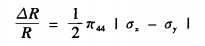
Secondly, we calculated the film thickness ratio (overlay thickness: bulk silicon strain film thickness) from 0.002 to 0.5. The final result is shown in the figure.
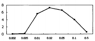
FIG. 1 Relation between film thickness ratio and relative error
4) Summary
It can be seen that when the thickness of the overlay is very thin, the relative error it can introduce is small. When the film thickness is large, the result of ANSYS division of elements will gradually approach the ideal state, and the final relative error will be reduced. Therefore, in the following simulation, a single layer membrane model can be used to approximate the real sensor.
4. Influence of strain film width-length ratio on theoretical output
1) Influence of strain film width-length ratio on theoretical output at fixed width
In this analysis, the width of the entire sensor is fixed at 5.2nlln, the width of the strain film is fixed at 2.22nlln, and the length is successively 1-5 times of the width. The thickness of strain film is 100 /.tm. The final calculation results are shown in Figure 2
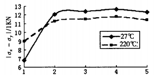
FIG. 2 I - I under different width and length ratios
It can be seen from these results that, when the length of one side is fixed, the theoretical output value of the sensor increases with the increase of the length of the other side, and begins to decline after the ratio exceeds 1:4. In particular, the segment from 1:1 to 1:2 increased the most. This is because when the length of one side is increased, the area of the strain film will increase accordingly, and the theoretical output value will naturally increase. However, it should be noted that the rate of increase of the theoretical output value gradually reaches saturation, so generally 1:2 can be done.
2) Influence of strain film width-length ratio on theoretical output under fixed area
In this analysis, the area of the whole sensor was fixed as 33.8- and the area of the strain film was fixed as 8.3028II. Then, the length and width of the sensor and the strain film were changed at the same time, so that the width and length ratio of the sensor and the strain film were 1:1 -- 1:5 respectively. The thickness of the variable film is 100 /. tm. The final calculation results are shown in Figure 3.
FIG. 3 Different aspect ratio of same area
It can be seen from FIG. 3 that when the strain film area is fixed, the theoretical output value of the sensor decreases with the increase of the width/length ratio, and the rate of decline is approximately linear (closer to linear at high temperature). Therefore, under the condition that the area of the sensor and its strain film is fixed, the square film should be made as far as possible so as to obtain the maximum theoretical output value. We further calculated the stress distribution on the surface of the square film, and the results are shown in Figure 4.
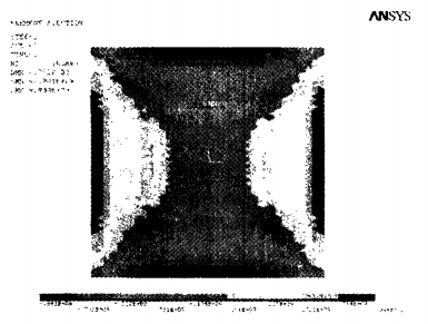
FIG. 4 Stress distribution on the surface of square film
It can be seen from Figure 4 that the maximum stress area on the surface of the square film pressure sensor is located at the edge of the strain film. For maximum output, the resistance should be placed in these four locations; This is consistent with the conclusion of previous theoretical analysis.
5. Influence of strain film thickness on theoretical output
The sensor model used in the above analysis has a length of 6.5 mm and a width of 5.2mill, a strain film length of 3.74nlln and a width of 2.22m/n, and a thickness ranging from 60 /.tm to 200 /.tm. Each increase of 20 /.tm makes one model, a total of 8 models. FIG. 5 shows the I-I value at =0 when the thickness is 100 /.tm:
As can be seen from FIG. 6, under the condition that the area of the strained film is fixed, the theoretical output value gradually decreases with the increase of film thickness and approximately presents a negative exponential decline. Therefore, if mechanical strength permits, the strain film should be thinned as much as possible to obtain a higher output value.
6 Actual measurement results
According to the optimized design, we made a series of pressure sensors and tested them. Constant current source power supply is used for testing, current intensity is 1mA, single-arm resistance is about 4kQ; Calculate the full scale output value according to the test results. In addition, the simulation value of the full-scale output is calculated by using the results of ANSYS simulation (the value is not 13.6X10). The test results are shown in Table 2 and Table 3: (The unit of simulated value and actual output is mv/(mA·MPa)
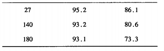
Table 2 Simulated values and actual output values of a sensor with a film thickness of 125 m
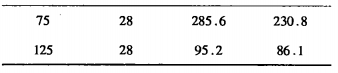
Table 3 Simulation and actual output values of sensors with different film thickness from 28 to C
Considering the simplification of the simulation model, the realization of each part in manufacturing and the theoretical situation are different, and the position of the resistance placed on the actual sensor cannot be accurately located in the theoretical position, so the actual output value is bound to be less than the theoretical value. It can be seen from the above results that the actual values are in good agreement with the theoretical values.
7 Conclusion
In this paper, a series of analysis and modeling of SOI monocrystalline silicon pressure sensor are carried out by using finite element analysis method and ANSYS software. From these simulations and analyses, the following conclusions can be drawn:
1) Under the general simulation accuracy requirements and technological conditions, it is feasible to ignore other components on the surface of the silicon pressure sensor;
2) To obtain the maximum output of the sensor:
(1) When the length of one side of the strain film is fixed, the length of the other side should be appropriately increased, but usually the length of the other side is 2 times of the length of the fixed side.
(2) When the area of the strain film is fixed, the stress film should be square.
3) Under the condition of mechanical strength, the thinner the stress film, the larger the output;
4) From the measurement results of the SOI monocrystalline silicon pressure sensor optimized according to the simulation results, the theory is in good agreement with the practice. The SOI monocrystalline silicon pressure sensor designed and developed by us has the characteristics of high sensitivity and high operating temperature. It is a kind of high temperature pressure sensor with broad application prospect.
Reference literature
[1] Zhang Tongsheng, Zhang Fude. Simple finite element method and its application [M]. Seismological Press, 1990:1 -- 102
[2] http://www.memsnet.org/materials
[3] Semiconductor sensor [M]. Tianjin University Press, 1990:156 -- 204