


Research and development of high temperature piezoresistive pressure sensor
1 Introduction
As the main product of MEMS, pressure sensor, especially high temperature pressure sensor, has a wide range of applications (1). Typical high temperature pressure sensors are high temperature piezoresistive pressure sensor, quartz pressure sensor, sputtering alloy thin film high temperature pressure sensor, ceramic thick film high temperature pressure sensor (2), optical fiber high temperature pressure sensor, diamond pressure sensor, etc., they have their own characteristics and shortcomings, the use of different environments, high temperature piezoresistive pressure sensor because of its advanced production technology, Compatible with semiconductor integrated circuit planar process, easy to realize systematization, intelligent, in line with the development direction of sensors. (3)
The traditional silicon diffusion piezoresistive pressure sensor uses four heavily doped P-type silicon strain resistors to form the force-sensitive detection mode (4) of Whiston Bridge, and adopts PN junction isolation. When the temperature is above 100℃, the leakage current of PN junction is very large, so that the device cannot work. Therefore, the easier way to design and manufacture high temperature piezoresistive pressure sensor is to cancel the isolation of monocrystalline silicon PN junction.
2 Polysilicon medium and high temperature pressure sensor
Polycrystalline silicon thin films with low pressure vapor phase deposition method LPCVD owpres - surechemicalvapordeposition (1) preparation on Si02 or Si3N4, forming force sensitive material, using the ion implantation doping, strain testing bridge. Polysilicon pressure sensor is located at low cost, medium operating temperature and medium sensitivity L5j5(compared with the single crystal pressure sensor with the same design parameters, the sensitivity is only 1/4 to 1/5), and its transverse piezoresistive coefficient is much smaller than the longitudinal piezoresistive coefficient, so the design can only make full use of positive and negative longitudinal stresses. There are a large number of suspension bonds in the grain boundary of polysilicon chips, which capture hydrogen ions during the film formation, and hydrogen ions have a large amount of unbinding ability in the non-hydrogen-rich environment at high temperature, so it is difficult to solve the problem of high temperature performance stability. Figure 1 is a typical design of a polycrystalline silicon high temperature pressure sensor.
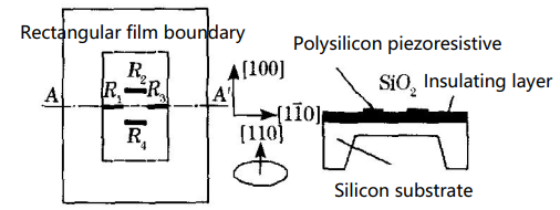
Figure 1. Typical design of polycrystalline silicon high-temperature pressure sensor
3.1 Only (6H) one SiC high temperature pressure sensor
As shown in FIG. 2, use N-type 6H -- SiC single crystal as the substrate, epitaxial P-type and N-type 6H -- SiC on it, and use P-type 6H -- SiC in the middle as the etching stop layer. Make a varsion-sensitive resistor by electrochemical etching PEC(photoelectrochemical etching) N-type 6H -- SiC. si02 is then deposited on the surface, and finally contact holes are carved to deposit metal and metallize to form ohmic contacts. a(6H) SiC high temperature pressure sensor uses a SiCPN junction of 6h-sic material with wide band gap and low hole mobility to replace the transmission of silicon PN junction isolation, and improves the working temperature of the sensor. KULflE, an American company, used a SiCPN junction to increase the operating temperature of the sensor to 500℃. The sensitivity of I6j is 0.58mV/V/MPa at 500℃ and 1.17mV/V/MPa at room temperature. The full-scale non-linearity and hysteresis are 1 0.17% and 0.17%, respectively. There are no relevant reports in China.
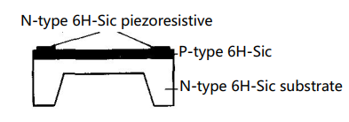
Figure 2 (6H) A SiC sensor chip
3.2 3C -- SiC high temperature pressure sensor
The 3C -- SiC high temperature pressure sensor uses the SOI(SiliconoilInsula-Tor) wafer as the substrate to selectively grow 3C -- SiC on the sio2 surface of the mask layer. The 3C -- SiC only deposits in the part in contact with si to form the 3C -- SiC varistor strip. The sensor developed by Daimler-Benz Technology Research Center in Germany in collaboration with the Technical University of Berlin uses a circular membrane structure to achieve a high sensitivity of 21mV/V/MPa at 200℃ and 35mV/V/MPa at room temperature. It is considered that the operating temperature of SiC can be raised to 450℃ because of its excellent piezoresistive effect. [7] During the Ninth Five-Year Plan period, domestic technicians carried out research on the growth and analysis of silicon carbide thin film material on si and the fabrication of piezoresistive pressure sensor. The high quality 3C -- SiC film on si was obtained by the transition buffer layer growth technology, and the SiC piezoresistive high temperature and high pressure sensor was made, including the medium pressure sensor made of the preferred 3C -- SiC polycrystalline film on Si02 / si and the high pressure sensor made of the single crystal 3C -- sic film on si. Failed to solve the packaging problem to achieve 200℃ sample stopped. (8)
4 Monocrystalline silicon SO1 high temperature pressure sensor
The two basic SOl wafer structures using the silicon oxide insulator SOl (9) technology are shown in Figure 3. The fabrication method is siliconon the insulator, such as silicon and sapphire SOS technology. Another for buried insulating Silicon and silicon layer on the surface of the body in the body, such as silicon/silicon bonding SDB (siliconwaferdirectbonding) LlO] technology and SIMOX (separationbyimplantedoxygen) _l technology, etc., SDB technology is combined with back etching to form BESOI technology, and SMARTCUT(or UNIBOND)12 technology is formed when combined with hydrogen ion injection, and ELTRAN(epitaxial layertransfer)13 technology based on the features of multi-postale silicon
Other methods for making SOI chips include RMR(zone. meltingre). Crystallization), SEG/ELO (selectiveepitaxial growthand epitaxiallateralovergrowth) (14). The common methods for providing commercial SOI chips are BESOI, SMARTCUT, and SIMOXll (15).
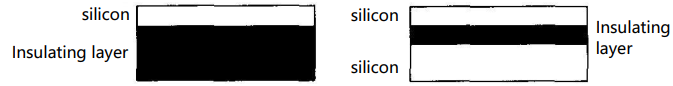
(a) Silicon on the bulk insulator (b) the insulator is buried between the bulk silicon and the silicon layer
Figure 3. Two basic SOl chip structures
4.1 BESOI Technology
As shown in FIG. 4, an l layer of N-type silicon film is epitaxial on the P-type (100) silicon substrate, and the cavity is corroded by anisotropy on the other N-type (100) silicon film, and then the two silicon wafers are bonded. P-type substrate was corroded by PN self-stop etching method, and electrical resistance was formed by double-sided lithography and ion implantation. The silicon on the back is removed by polishing method according to the size required by the design to form the required structure. Its main advantages are simple process, good silicon film quality, good SiO: layer performance and easy to control the thickness, the disadvantage is that each bonding cost two silicon wafers, it is difficult to obtain a uniform ultra-thin silicon film.
After years of development, KULrrE has developed ultra-high temperature pressure sensors, such as XTEH-10Lac-190 (M) series, with the BESOI technology of si02 medium isolation. The operating temperature is -55 ~ 482℃. At present, the domestic technology has been mature, the temperature resistance is 200℃ as the upper limit, the chip manufacturing method and sensor manufacturing method of authorized patents see literature 16-17.
After years of development, KULrrE has developed ultra-high temperature pressure sensors, such as XTEH-10Lac-190 (M) series, with the BESOI technology of si02 medium isolation. The operating temperature is -55 ~ 482℃. At present, the domestic technology has been mature, the temperature resistance is 200℃ as the upper limit, the chip manufacturing method and sensor manufacturing method of authorized patents see literature 16-17.
4.2 SMARTCUT Technology
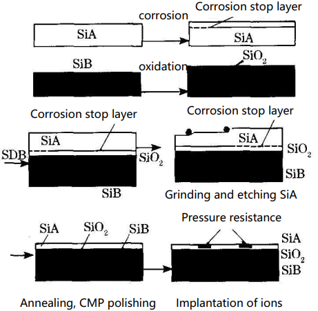
SMARTCUT technology is to inject a moderate dose of hydrogen ions into one silicon wafer, and then bond with another silicon wafer at a low temperature. After heat treatment, the silicon/silicon bond pair splits at the projected range of the hydrogen ion injection. One piece forms an SOI structure, and the other piece of silicon can be recycled. This technology does not require corrosion, provides better chip quality and insulation layer, silicon film and embedded oxide layer can be adjusted, low cost, suitable for mass production. The main technological process is shown in Figure 5.
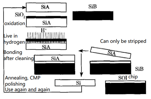
The sensor produced by this technology can withstand temperature up to 150℃, and the sensitivity is 63mv/(MPa·5v). It is estimated that the operating temperature can be increased to 300℃ by improving the packaging process. (18)
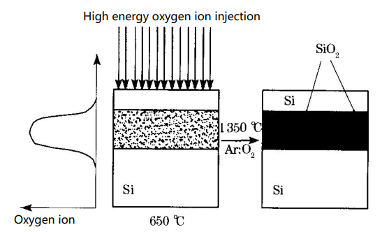
4.3 SIMOX technology
As shown in Figure 6, SIMOX technology is adopted to inject human oxygen ions on N-type silicon wafers at high energy to obtain high quality commercial SiO2 dielectric isolated SOI wafers, and MEMS process is used to produce high temperature resistant chips on the micro-machining platform.
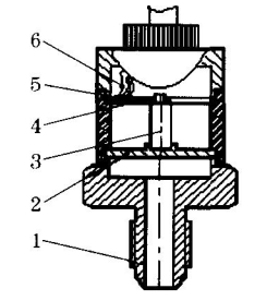
The SOI chip using SIMOX technology uses a cantilever beam isolation structure to isolate the measured high temperature fluid (or gas) from the silicon sensitive element to avoid the instantaneous high temperature impact of the measured object, and solves the problem of 2kC instantaneous high temperature impact. The performance index of the sensor reaches the international advanced water subdivision, and the structure diagram is shown in Figure 7.
Aiming at the low cost and serialization, the research results are commercialized, and the universal high temperature and pressure sensor is developed. The product has also reached the advanced water sub-class of the international similar products. [20]
5 Prospect of high temperature piezoresistive pressure sensor
There are two factors restricting the development of high temperature pressure sensor: chip quality and high temperature resistant packaging technology. Due to the micro-machining deviation of MEMS process, the consistency of force sensing element is poor, which brings great difficulty to the compensation of temperature drift in the later stage, and restricts the improvement of static accuracy and dynamic response ability of sensor. Therefore, it is necessary to analyze and feedback the initial test data of the chip, so that the production process becomes more mature and the yield increases. In the packaging process, the method of glass slurry sintering at low temperature is used to combine the chip and the elastic element as one, as shown in Figure 7 8[20] adopted the chip/glass ring electrostatic bonding technology, and then bonded with high temperature adhesive. In both processes, the matching of thermal expansion coefficient between materials and the elimination of stress should be solved, so as to further expand the operating temperature, improve the stability, and achieve low cost. In addition, in terms of structure, according to the requirements of various industries, the corresponding processing circuit is solved through modeling and analysis, so as to expand the application field of products, such as replacing the high-temperature melt pressure sensor [21], so as to standardize and serialize the products.
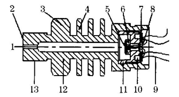
1 intake (or liquid) port :2 a flat head interface :3 a locking nut :4- heat sink :5 a silicon chip; 6 a glass ring; 7 a high temperature resistant circuit board; A piece of gold; 9 a wire 10 a locking hole :11 a stainless steel inner buckle; 12 - stainless steel base :13 - connection thread
Figure 8 General high temperature pressure sensor structure diagram
6 Closing Remarks
High temperature pressure sensor is widely used in aerospace, petrochemical, automotive and other fields of high temperature environment pressure measurement, has a great application prospect. Foreign high temperature and pressure sensors monopolize the international market for a long time. With the improvement of domestic MEMS process level and the breakthrough in the integrated design of sensitive components and sensor structure design, it is bound to have a place in this high-tech field.
References
[1] WERNER M, FAHRNER W, Review on materials, Micro sensorsytems, and device for high temperature and harsh environment applications, IEEE Transactions on Industrial Electronics, 2001, 48 (2): 249.257
[2]AYERDI I,CASTANO E,GARCIA A, et al. High tempere ceramic pressure sensor. Sens Actuator ,1997 ,A(60)72 - 75
[3]MIDDELHOEK S. Celebration of the tenth transducers conference: thepast , present and future research and development, Sens Actuators , 2000, (82); 2 minus 23.
[4]BA0 M. Mecro Mechanical Transducers-pressure Sensors, Acceleromneterand Gyroscopes .Dutch Amsterdam Publisher,2000:254 - 256
[5]OBIETA I,GASTANO E,CRACIA F.High temperature polysilicon pressure micro sensor. Sens actuator, 1995,A(46/47); 161-165
[6]OKOJIE R.Operation of a (6H)-SiC pressure sensor at 500 C .Sens Actuator, 1998,A(66):200 - 204.
[7]EICKHOFF M,MOLLER H, KROEETA G, et al.A high temperaturepressure sensor prepared by selective deposition of cubic on SOl sub.strates. Sens Actuators , 1999 ,A(74): 56 - 59.
[8] Zhu Zuoyun, Li Yuejin, Yang Yintang, et al. SiC thin film high temperature pressure sensor Sensor Technology,2001,20(2); 1-3
[9] PIOBL A,KRAUTER G.Samicon-on-insulator :material aspects and applications.Solid-state Electron, 2000,44:775-782.
[10] GOSELE U,REICHE M,TONG O.perties of SIMOX and bonded SOlmaterial. Microelectronic Engineering, 1995, 28:391-397.
[11] DIEM B, REY P,RENARD S,et al,SOI SIMOX: from bulk to surfacemicromachining and a new age for silicon sensors and actuators . Sens Actuators,1995,A(46/47):8 - 16.
[12] DU J,KO W,YOUNG D.Single crystal silicon MEMS fabrication basecon smart-cut technique.Sens Actuators,2004, A(112): 116-121.
[13] XIE XLIU WMEN C,et al, Fabrication of silicon-on-insulator-multilayer structure by epitaxial laver transfer. Physica B2003336(3).34- 349.
[14] KIYOFUMI S,TAKAO Y SOI wafers based on epitaxial technology.Solid State Technology,2000,43 (6) : 88-92.
[15] WANG X, CHEN M, CHEN J, et al. Nove approaches for low cost fabrication of SOl. Current Appl Phys, 2001, 1: 225-231.
[16] Zhang Xuan-xiong, LU De-Ren, WANG Wen-xiang, et al., Production Method of High Temperature and Pressure Sensor Chips,ZL99124237.8, 2002-11-20, China Patent
[17] Zhang Xuanxiong, Lu Deren, Wang Wenxiang, et al. Chinese Patent,ZL99124238.6, 2003-08-27. Production Method of High Temperature Ultra-High Pressure Pressure Sensor on Silicon Insulator.
[18] Huang Yiping, Zhu Shichang, Li Aizhen, et al. Intelligent stripping SOI high temperature pressure sensor. Journal of Semiconductors,2001, 22(7):924 - 927.[19]ZHAO Y,ZHAO L,JIANG Z. A novel high temperature sensor on the basis of SOI layers ,Sens. Actuators ,2003,A( 108); 108 minus 111.
[20] Wang Quan, Ding Jianning, Wang Wenxiang, et al. Research on packaging technology of general high temperature resistant miniature pressure sensor. Instrument Technique and Sensor, 2005(6):6-7.[21]TANAKA T,BAUER F,LUTZ T, etal. Liquid metal integrated test sys
tem (LIMITS) . Fusion Engineering and Design, 2004 ,72 : 83 - 92.
Recommended sensor: PTM300G high temperature pressure transmitter